- 取得連結
- X
- 以電子郵件傳送
- 其他應用程式

Electroplating Nickel Film
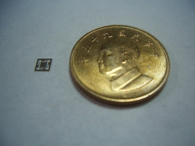
We based on the MEMS process to electroplate nickel film on silicon wafer. The figure was show the accelerometer dimension, it was very tiny structure.
The fabrication process step was show below:
a) Clean silicon wafer
b) Deposition chromium (Cr) on the silicon wafer
c) Coating photoresister (PR) on the silicon wafer
d) Photolithography pattern
e) Electroplating nickel (Ni)
f) Release PR
留言